Carnegie Mellon University and the Chinese University of Hong Kong researchers have devised a method for fabricating ultrahigh-resolution, complex 3D nanostructures out of diverse materials. Yongxin (Leon) Zhao of Carnegie Mellon University and Shih-Chi Chen of the Chinese University of Hong Kong have a major concept for producing nanodevices.
Zhao’s Biophotonics Lab is dedicated to the development of innovative approaches for studying biological and pathological processes in cells and tissues. The group uses expansion microscopy to enhance ways for proportionately enlarging tiny samples embedded in a hydrogel, enabling researchers to observe fine details without updating their microscopes.
An exciting interaction with Shih-Chi Chen, a professor from the Chinese University of Hong Kong’s Department of Mechanical and Automation Engineering, who was visiting Carnegie Mellon as an invited speaker in 2019, spurred a partnership between the two scholars. They believed they could utilise their combined skills to discover fresh solutions to a long-standing difficulty in microfabrication: shrinking the size of printed nanodevices to tens of nanometers or several atoms thick. Their answer is the inverse of expansion microscopy: build a material’s 3D pattern in hydrogel and compress it for nanoscale precision.
“Shih-Chi is well-known for developing the ultrafast two-photon lithography technology,” Zhao, the Eberly Family Career Development Associate Professor of Biological Sciences, stated. “We met at Carnegie Mellon during his visit and agreed to combine our approaches and abilities to explore this bold notion.”
The collaboration’s findings, which were published in the journal Science, offer up new avenues for the development of complex nanodevices.
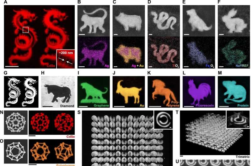
While traditional 3D nanoscale printers focus a laser point to serially process materials and take a long time to complete a design, Chen’s invention changes the width of the laser’s pulse to form patterned light sheets, allowing a whole image containing hundreds of thousands of pixels (voxels) to be printed at once without sacrificing axial resolution.
The manufacturing technology is known as FP-TPL (femtosecond project two-photon lithography). The process is up to 1,000 times quicker than prior nanoprinting methods and might pave the way for low-cost large-scale nanoprinting in biology, photonics, or nanodevices. The femtosecond two-photon laser would be used to adjust the network structure and pore size of the hydrogel, which would subsequently form boundaries for water-dispersible molecules. The hydrogel would next be submerged in water containing metal, alloy, diamond, molecular crystals, polymers, or fountain pen ink nanoparticles.
“By chance, all of the nanomaterials we attempted were naturally attracted to the printed pattern in hydrogel and assembled wonderfully,” Zhao added. “As the gel shrinks and dehydrates, the components become more densely packed and link.”
When a printed hydrogel is immersed in a silver nanoparticle solution, the silver nanoparticles self-assemble following the laser-printed pattern. The gel may shrink to up to 13 times its original size when it dries, making the silver dense enough to form a nano silver wire and transmit electricity, according to Zhao. Because the gels are three-dimensional, printed designs may also be three-dimensional.
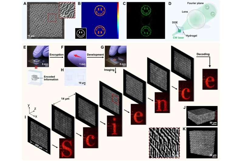
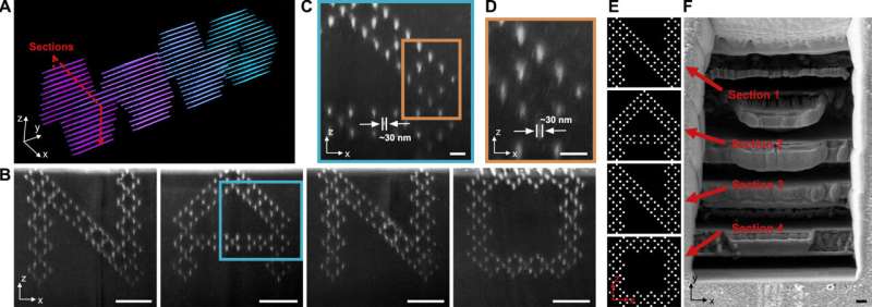
The researchers devised and produced a seven-layer 3D nanostructure that read “SCIENCE” after being optically decrypted as a demonstration of the technique’s applicability for encrypted optical storage—such as how CDs and DVDs are recorded and read using a laser. Each layer featured a 200×200-pixel letter hologram. Under an optical microscope, the whole structure appears as a transparent rectangle when the sample is shrunk. To read the information, one would need to know how much to enlarge the sample and where to shine a light through.
“According to our findings, the technology can store 5 petabits of data in a small cubic centimetre of area. That is nearly 2.5 times the total number of academic research libraries in the United States “He said.
Zhao said that the researchers’ long-term objective is to create functioning nanodevices made of different materials.
“Ultimately, we want to employ the new approach to construct functioning nanodevices such as nanocircuits, nanobiosensors, and even nanorobots for various purposes,” Zhao added. “Our only limitation is our imagination.”