Finding a material that might replace silicon is a critical task in the realm of nanoelectronics. For many years, graphene has seemed promising. However, because of destructive processing techniques and the absence of a new electronics paradigm to accept it, its potential has been compromised along the way. The need for the next major nanoelectronics platform is greater than ever, since silicon is almost at its limit in terms of supporting faster computation.
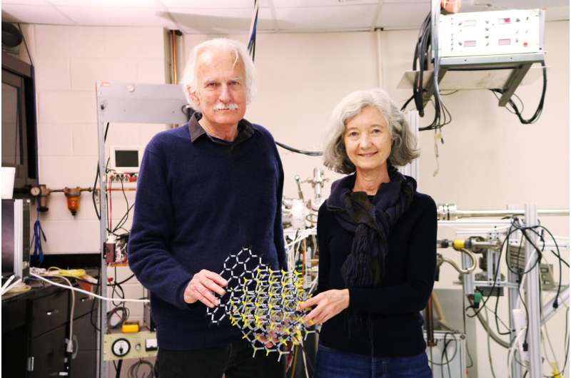
Walter de Heer, Regents’ Professor in the School of Physics at Georgia Tech, has made a significant advancement in the argument for silicon’s replacement. A brand-new nanoelectronics platform based on graphene, a single sheet of carbon atoms, has been created by De Heer and his associates. Any silicon substitute that is practical must be compatible with traditional microelectronics production.
The team’s study, which was published in Nature Communications, may also have led to the discovery of a brand-new quasiparticle. Their finding may have an impact on quantum and high-performance computing, as well as the production of smaller, quicker, more efficient, and environmentally friendly computer processors.
De Heer said that the strength of graphene’s chemical bonds, which hold its flat, two-dimensional structure together, is what gives it its power. “It was immediately apparent that graphene can be downsized considerably more than silicon can, allowing for much smaller devices that operate at faster speeds and generate a lot less heat. In theory, this allows for the packing of more devices onto a single graphene chip than silicon can.”
Epitaxial graphene, also known as epigraphene, is a layer of graphene that was discovered to spontaneously grow on top of silicon carbide crystal, a semiconductor utilised in high power electronics. De Heer presented this alternate type of electronics in 2001. At the time, scientists discovered that graphene devices could be linked without the need of metal wires and that electric currents flow without resistance around the edges of epigraphene. A kind of electronics based on the distinct light-like characteristics of graphene electrons is made possible by this combination.
We anticipate comparable results in epigraphene ribbons and networks, according to de Heer, who noted that quantum interference has been detected in carbon nanotubes at low temperatures. With silicon, “this crucial property of graphene is not feasible.”
constructing the platform
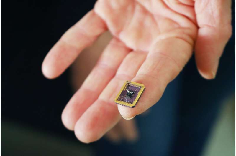
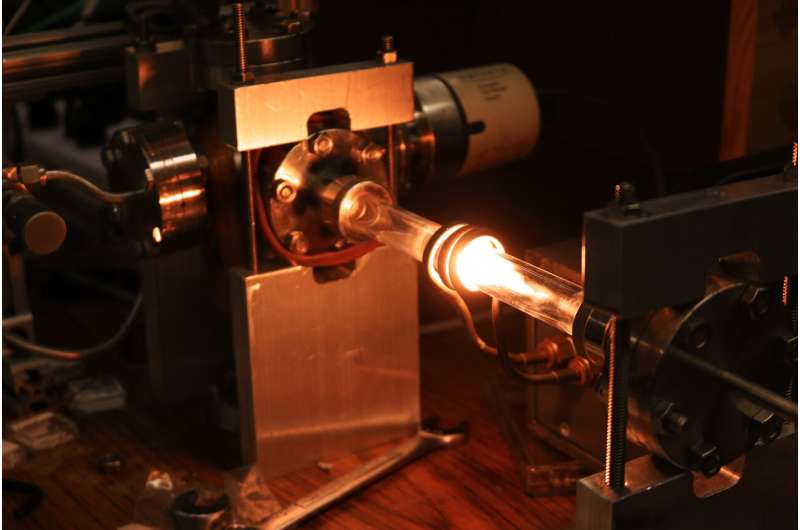
The scientists produced a modified version of epigraphene on a silicon carbide crystal substrate to produce the novel nanoelectronics platform. They created distinctive silicon carbide chips using electronics-grade silicon carbide crystals in partnership with scientists at the Tianjin International Center for Nanoparticles and Nanosystems at the University of Tianjin, China. Using proprietary furnaces, the graphene was generated in de Heer’s Georgia Tech lab.
The researchers carved the graphene nanostructures and welded their edges to the silicon carbide chips using electron beam lithography, a technique often used in microelectronics. The graphene’s edges, which in the absence of this procedure would react with oxygen and other gases and perhaps obstruct the migration of the charges along the edge, are mechanically stabilised and sealed. Last but not least, the researchers employed a cryogenic equipment to record the electrical characteristics of their graphene platform from a near-zero temperature to ambient temperature.
looking at the edge state
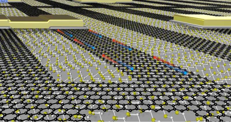
The scientists found that the electric charges in the graphene edge state resembled photons in an optical fibre, which are capable of travelling across great distances without scattering. They discovered that the charges moved down the edge for tens of thousands of nanometers before dispersing. In earlier applications, graphene electrons could only go around 10 nanometers before encountering minute flaws and dispersing in various directions.
According to Claire Berger, a physics professor at Georgia Tech and the director of research at the French National Center for Scientific Research in Grenoble, France, “what’s special about the electric charges in the edges is that they stay on the edge and keep on going at the same speed, even if the edges are not perfectly straight.”
Electrons with a negative charge are what carry electrical currents in metals. However, the researchers’ tests revealed that the edge currents were not carried by electrons or holes, in contrast to their assumptions (a term for positive quasiparticles indicating the absence of an electron). Instead, an extremely uncommon quasiparticle that has no charge and no energy but nevertheless flows without resistance was responsible for carrying the currents. Despite being a single item, the hybrid quasiparticle’s components were shown to move on different sides of the graphene’s edges.
The peculiar characteristics suggest that the quasiparticle could be the elusive Majorana fermion, which Italian theoretical physicist Ettore Majorana predicted in 1937, which physicists have been hoping to use for decades. The creation of electronics employing this novel quasiparticle in flawlessly linked graphene networks is revolutionary, according to de Heer.
According to de Heer, it will probably be another five to ten years before we see the first graphene-based devices. But now that the team has developed a new platform for epitaxial graphene, technology is closer than ever to naming graphene the silicon’s replacement.