Although multiple studies have reported promising properties of prototype devices using two-dimensional materials for sensing and driving electrical current, the technology readiness level of these materials remains low due to several factors. One of the main issues is that the synthesis and processing methods used are not compatible with industry standards. Additionally, the devices are often created on unfunctional substrates, leading to poor variability and yield. As a result, significant improvements are needed before these materials can revolutionize the semiconductor industry.
Dr. Mario Lanza, an associate professor of materials science and engineering at King Abdullah University of Science and Technology (KAUST), has led a team of scientists to successfully integrate two-dimensional materials onto silicon microchips. This achievement resulted in excellent integration density, electronic performance, and yield, and has been published in the journal Nature.
“In the future, most microchips will exploit some of the many outstanding electronic and thermal properties of these materials,” said Lanza.
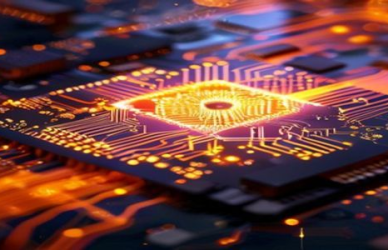
Dr. Mario Lanza’s team at King Abdullah University of Science and Technology has developed a groundbreaking approach to integrate two-dimensional materials onto silicon microchips. The team utilized multilayer hexagonal boron nitride, a two-dimensional insulating material with a thickness of about 6 nanometers. They incorporated this material onto microchips containing silicon transistors of complementary metal-oxide-semiconductor (CMOS) technology, which is present in many electronic products like phones, computers, automobiles, and household appliances.
The hybrid 2D/CMOS microchips produced by the team exhibited exceptional durability and unique electronic properties that enabled the creation of artificial neural networks with extremely low power consumption. These microchips can compute spiking neural networks, which are crucial components of the current artificial intelligence systems that are in high demand. Current devices are not ideal for implementing this type of neural network, and there is a market need to find new approaches.
The successful integration of 2D materials onto silicon microchips has piqued the interest of several semiconductor companies. This development could help other companies reduce processing costs and energy usage, which are crucial factors in the field of microchip manufacturing and artificial intelligence. Many companies in this field are striving to create new hardware that can decrease data processing time and energy consumption, but they have yet to find a suitable device.
IBM has attempted to integrate graphene into transistors for radio-frequency applications, but the devices were not capable of storing or processing information. In contrast, the devices created by Dr. Lanza’s team are only 260 nanometers in size and can be made much smaller if more advanced microchips become available.
The potential for far-reaching industry applications and the high performance of the devices and circuits produced make this work extremely exciting for the field of nanoelectronics and semiconductors.
You might also be interested in reading, Glaze Software Helps Protect Artists from AI-generated Replication